SEM vs TEM: Which is right for you?
Two widely used microscopy techniques are Scanning Electron Microscopy (SEM) and Transmission Electron Microscopy (TEM). While both use electron beams to generate images at high resolutions, their applications, capabilities, and limitations differ significantly.
Choosing the right method depends on your specific research goals, sample type, and the level of detail required. It may also depend on what your lab has available.
Understanding SEM and TEM
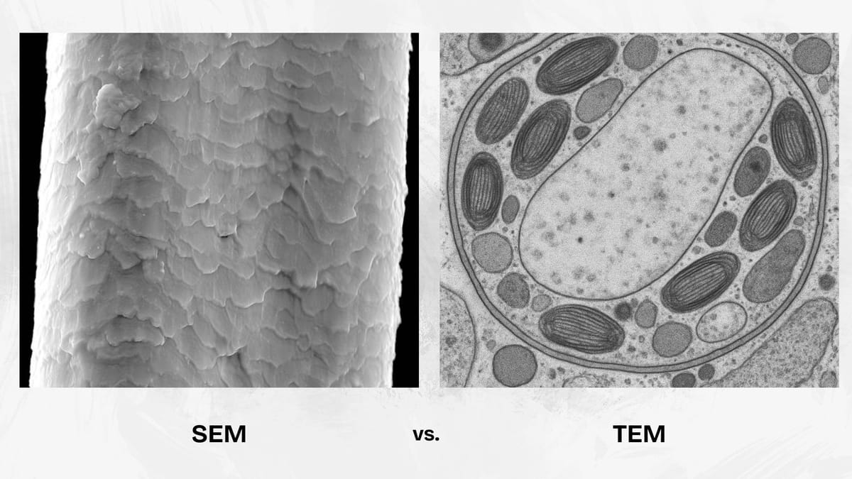
SEM scans a focused beam of electrons across a sample’s surface. The electrons interact with atoms in the sample, producing various signals that reveal surface topography and composition. Two detectors are in place to detect the two types of imaging electrons: backscattered electrons (BSE) from source electrons refclecting off the sample surface, and secondary electrons (SE), which originate from the sample's atoms due to introduction of the electron beam.
In TEM, however, electrons are detected after they pass through an ultra-thin sample. The interactions between the electrons and the sample produce high-resolution images revealing internal structures. TEM images are typically two-dimensional but may offer greater resolution than SEM depending on your sample.
When to Choose SEM
SEM is a good selection when your primary interest is to examine the topography of your sample, such as texture or particle shape. During my time in graduate school, I used SEM to examine pieces of metals from my thesis research. One of my colleagues collected a series of SEM images of fabric following her thesis experiments to examine how a certain chemical affected the material.
It also works well with biological samples (with preparation), or microelectronics. SEM is user-friendly and quite fast in terms of both setup and imaging, making it a common tool in academia, research & development, quality control and industrial applications.
Best for:
- Topographic imaging
- Surface coatings and defect examination
- Particulate analysis and sizing
- Moderate to high resolution needs
When to Choose TEM
TEM is your go-to for atomic-level detail or examining internal structures. It's ideal when studying crystallography and understanding cellular structure. However, the preparation process is more labor-intensive and requires precision in sample thinning.
Best for:
- Nano-materials and lattice structures
- Defect and interface studies
- Bio-molecular structure
- High-resolution imaging
Final Thoughts
Both SEM and TEM are powerful instruments, each excelling in different areas. If you're focused on surface detail and need a faster, more accessible method, SEM is likely the better choice. If your research requires ultra-high resolution and insight into internal structures or crystallography, I recommend working using TEM.
Ultimately, your choice should align with your scientific questions, available resources, and the level of detail your study demands.
Thanks for reading!
Feel free to contact Chemistry Weekly at ChemistryWeeklyNews@gmail.com with any questions or comments.
Disclosure
The information above is based on my own beliefs, opinion and experiences. In no way does this blog represent or reflect the schools I have been to or the companies that I work and/or have worked for. I am not responsible or liable for any events that occur as a result of this information.
I am not affiliated with any of the companies mentioned above.